Canon has filed a patent application (publication number P2026052804, published March 25, 2026, filed September…
Canon patent for electrically bending image sensor
Indefatigable Canon Labs produced a new, innovative patent, an image sensor that bends when electricity is applied. Such a sensor would allow for optics with larger apertures, and also reduces light falloff at the edges that’s typical for flat CMOS sensors. This is not the first Canon patent for a curved sensor.
- Patent publication number 2016-201425
- Release date 2016.12.1
- Application date 2015.4.8
- Canon patent
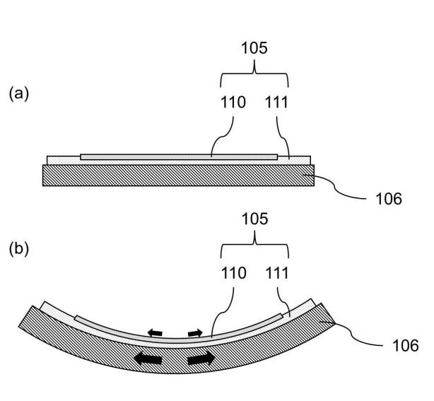
- Coupling the imaging element and the expansion / contraction section
- As the stretchable portion expands, the amount of curvature of the imaging surface increases
- The expansion and contraction section is electrically controlled
Excerpt from the patent literature:
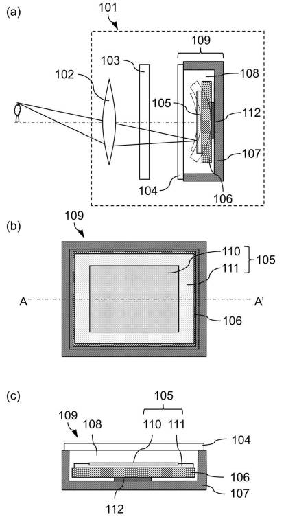
[Claim(s)] [Claim 1] An image sensor which has the 2nd page of an opposite side in the 1st page including an imaging region and said 1st page,It is an imaging device provided with an elastic member combined with said 2nd page of the aforementioned image sensor,
The aforementioned elastic member can respond to an electrical signal input into the aforementioned elastic member, and it can expand and contract it over said 2nd page,
An imaging device characterized by said curved quantity of the 1st page enlarging as the aforementioned elastic member develops over said 2nd page.
[Claim 2] The aforementioned elastic member,
A plate-like elastic section,
A first electrode that was arranged at the aforementioned image sensor side to the aforementioned elastic section,
With the aforementioned image sensor side, a second electrode which was arranged at an opposite side is included to the aforementioned elastic section,
In plane view over said 1st page, said first electrode and said second electrode are arranged so that it may lap with the aforementioned imaging region at least among the aforementioned image sensors,
The imaging device according to claim 1, wherein it responds to voltage applied between said first electrode and said second electrode and the aforementioned elastic section expands and contracts over said 2nd page.
[Claim 3] The imaging device according to claim 1 or 2, wherein it expands [ the aforementioned elastic member ] and contracts radiately from a center of the aforementioned elastic member over said 2nd page in plane view over said 1st page.
[Claim 4] In plane view over said 1st page, the aforementioned imaging region has the rectangular shape which has a long side and a shorter side,
The imaging device according to claim 1 or 2, wherein the aforementioned elastic member expands and contracts in the direction of the aforementioned long side.
[Claim 5] The aforementioned imaging device further contains a substrate for mounting the aforementioned image sensor,
The aforementioned elastic member is combined with the aforementioned substrate via a coupling member,
An imaging device of a description in any 1 item of Claims 1-4 having a circle configuration to which the aforementioned coupling member laps in the center of the aforementioned imaging region in plane view over said 1st page.
[Claim 6] The aforementioned imaging device further contains a substrate for mounting the aforementioned image sensor,
The aforementioned elastic member is combined with the aforementioned substrate via a coupling member,
The imaging device according to claim 4 having the outline to which the aforementioned coupling member was along said side of the 1st page in plane view over said 1st page.
[Claim 7] An imaging device of a description in any 1 item of Claims 1-4, wherein the aforementioned elastic member is a substrate for mounting the aforementioned image sensor.
[Claim 8] An imaging device of a description in any 1 item of Claims 1-7, wherein the aforementioned elastic member is a piezoelectric device.
[Claim 9] An imaging device of a description in any 1 item of Claims 1-8, wherein thickness of a semiconductor layer at which a photoelectric conversion part of the aforementioned image sensor was arranged is 100 micrometers or less and distance of a semiconductor layer and the aforementioned elastic member at which a photoelectric conversion part of the aforementioned image sensor was arranged is 1000 micrometers or less.
[Claim 10] An imaging device of a description in any 1 item of Claims 1-9, wherein black resin is arranged between the aforementioned elastic member and the aforementioned image sensor.
[Claim 11] An imaging device of a description in any 1 item of Claims 1-10 to which the aforementioned image sensor and the aforementioned elastic member are characterized by having combined with each other in a region with which the aforementioned imaging region and the aforementioned elastic member lap at least among the aforementioned image sensors in plane view over said 1st page.
[Claim 12] An imaging device of a description in any 1 item of Claims 1-11 to which a product of Young’s modulus of the aforementioned image sensor and a cube of thickness is characterized by being smaller than a product of Young’s modulus of the aforementioned elastic member, and a cube of thickness.
[Claim 13] An imaging device of a description in any 1 item of Claims 1-12 to which a coefficient of linear expansion of the aforementioned image sensor and a coefficient of linear expansion of the aforementioned elastic member are characterized by a mutually equal thing.
[Claim 14] The aforementioned image sensor has a silicon layer,
An imaging device of a description in any 1 item of Claims 1-13, wherein coefficients of linear expansion of the aforementioned elastic member are 3.0 or more ppm/K and 4.0 ppm/K or less. [via Egami]
Related Posts