Canon has filed a patent application (publication number P2026052804, published March 25, 2026, filed September…
Canon patent for stacked sensor design (AF and image data off the sensor)
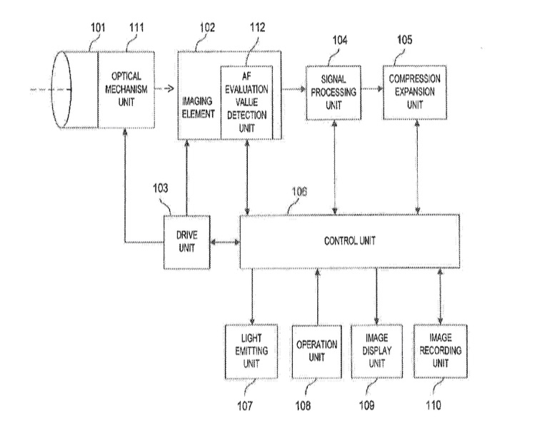 Canon patent application US20170366776 describes several stacked sensor designs.
The patent focuses on separating auto-focus and image data pipelines from the chip on the image sensor. Such a design has several advantages: less bandwidth to transfer data from the sensor, which leads to more speed and reduced power consumption (hence also less heat).
The patent abstract:
An imaging element having a layered structure including a first chip having a pixel portion in which pixels for photoelectrically converting an optical image of an object and generating a pixel signal are arranged two-dimensionally and a second chip in which a drive means of the pixel portion is arranged, and having a first output path to output the pixel signals of at least a first pixel group in the pixel portion and a second output path to output the pixel signals of a second pixel group, comprises the a conversion means for converting the pixel signals of the first and second output paths into digital signals and a control information generation means for generating control information of a photographing operation of the object by using the digital signal converted by the conversion means, wherein at least a part of the conversion means is arranged in the first chip.
Please note that patent applications do not mean a company will implement the described technology any time soon. Indeed, most patents never make it into production. An example of a Canon patent describing a technology that might be featured on a future Canon DSLR can be seen here, another one here.
Related Posts