Canon has filed a patent application (publication number P2026052804, published March 25, 2026, filed September…
Yet another Canon patent for a curved sensor design
Another Canon patent for a curved sensor design. The fourth if I am not wrong, previously: 1 | 2 | 3
- Patent publication number 2016-213571
- Release date 2016.12.15
- Application date 2015.4.30
- Canon patent
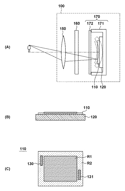
- Curved state based on the measurement result of the bending state to control the
- Measurement method is pressure sensor, laser light
For those who dare: after the break you can read a machine translated excerpt from the patent literature.
[via Egami] [Claim(s)] [Claim 1] It is an imaging device provided with an image sensor chip which has the picture element region where a plurality of pixels were arranged,A control part which controls a state of a curve of the aforementioned image sensor chip so that the aforementioned picture element region curves,
A measuring part which is arranged at adjacent spaces of the aforementioned picture element region in the aforementioned image sensor chip, and measures a state of a curve of the aforementioned image sensor chip,
It has a set part which sets up a target of a state of a curve of the aforementioned image sensor chip based on a state of an optical lens used for photographing,
The aforementioned control part controls a state of the aforementioned curve based on a result of having compared a target set [ aforementioned ] up with a state of the aforementioned curve measured [ aforementioned ].
An imaging device characterized by things.
[Claim 2] When a state of the aforementioned optical lens is changed, the aforementioned set part updates a target set [ aforementioned ] up based on a state of an optical lens in which the state was changed.
It is an imaging device to Claim 1 characterized by things.
[Claim 3] The aforementioned set part contains a memory which stores a reference table, and a selecting part which chooses a parameter corresponding to a state of the aforementioned optical lens with reference to the aforementioned reference table,
The aforementioned control part controls a state of the aforementioned curve based on a parameter chosen [ aforementioned ].
The imaging device according to claim 1 or 2 characterized by things.
[Claim 4] The aforementioned set part sets up a target of a state of the aforementioned curve based on a part number of an optical lens attached to the aforementioned imaging device.
An imaging device of a description in any 1 item of Claim 1 characterized by things to Claim 3.
[Claim 5] The aforementioned set part sets up a target of a state of the aforementioned curve based on a position of the aforementioned optical lens.
An imaging device of a description in any 1 item of Claim 1 characterized by things to Claim 4.
[Claim 6] The aforementioned measuring part contains a piezoresistance type pressure sensor.
An imaging device of a description in any 1 item of Claim 1 characterized by things to Claim 5.
[Claim 7] The aforementioned image sensor chip has a semiconductor substrate,
The aforementioned measuring part contains a diffused resistor formed in the aforementioned semiconductor substrate.
An imaging device of a description in any 1 item of Claim 1 characterized by things to Claim 6.
[Claim 8] In plane view over a top surface of the aforementioned image sensor chip, said plurality of sensors correspond to a plurality of sides which form an outer edge of the aforementioned image sensor chip including a sensor of plurality [ measuring part / aforementioned ], respectively.
An imaging device of a description in any 1 item of Claim 1 characterized by things to Claim 7.
[Claim 9] In the aforementioned plane view, the aforementioned image sensor chip has the rectangular shape which has a long side and a shorter side, and each of said plurality of sensors is formed in a form line along a long transverse direction.
An imaging device of a description to Claim 8 characterized by things.
[Claim 10] Each of said plurality of sensors is a resistance element, and said plurality of sensors form a bridged circuit.
The imaging device according to claim 8 or 9 characterized by things.
[Claim 11] The aforementioned measuring part contains a plurality of pixels of other which said plurality of pixels are several of other different pixels, and were arranged in the aforementioned adjacent spaces,
Each of said plurality of pixels forms an imaging pixel,
Each of said plurality of pixels of other forms an optical black pixel.
An imaging device of a description in any 1 item of Claim 1 characterized by things to Claim 5.
[Claim 12] The aforementioned measuring part is monitoring a band gap of a component which constitutes the aforementioned image sensor chip, and measures a state of the aforementioned curve based on a result of the monitor.
An imaging device of a description in any 1 item of Claim 1 characterized by things to Claim 5.
[Claim 13] It is an imaging device provided with an image sensor chip which has the picture element region where a plurality of pixels were arranged,
A control part which controls a state of a curve of the aforementioned image sensor chip so that the aforementioned picture element region curves,
A measuring part which measures a state of a curve of the aforementioned image sensor chip,
It has a set part which sets up a target of a state of a curve of the aforementioned image sensor chip based on a state of an optical lens used for photographing,
A laser beam irradiation part to which the aforementioned measuring part irradiates a laser beam to the aforementioned image sensor chip, A laser beam primary detecting element which detects a laser beam reflected by the aforementioned image sensor chip is included, and a state of a curve of the aforementioned image sensor chip is measured based on a detection position in the reflected aforementioned laser beam primary detecting element of a laser beam,
The aforementioned control part controls a state of the aforementioned curve based on a result of having compared a target set [ aforementioned ] up with a state of the aforementioned curve measured [ aforementioned ].
An imaging device characterized by things.
[Claim 14] It further has a light reflection section which is arranged at adjacent spaces of the aforementioned picture element region in the aforementioned image sensor chip, and reflects a laser beam from the aforementioned laser beam irradiation part.
The imaging device according to claim 13 characterized by things.
[Claim 15] In plane view over a top surface of the aforementioned image sensor chip, the aforementioned light reflection section is arranged at a corner area in the aforementioned image sensor chip.
The imaging device according to claim 14 characterized by things.
Related Posts