I guess many of us were waiting for this: the possibility to use Sigma's excellent…
Canon’s 250MP APS-H sensor presented at ISSCC 2016

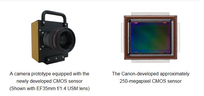
ISSCC 2016, the International Solid‑State Circuits Conference held in San Francisco, just closed its doors. This is a specialist conference about circuits technology, something Canon with their newly developed sensors would not miss for sure. Indeed, Canon presented their 250MP APS-H sensor, a piece of technology I reported a few times in the past.
The folks at Harvest Imaging posted a summary of the presented tech. About Canon’s 250MP sensor:
Hirofumi Totsuka of Canon presented a 250 Mpixel APS-H size imager : 1.5 um pixel pitch (4 sharing) made in 0.13 um technology node. The device is consuming 1.97 W at full resolution 5fps. An interesting build-in feature of this sensor is the following : ALL pixel signals are converted by column SS-ADCs with a single ramp, but in front of the ADC, each column has its own PGA that can be switched to 4x or 1x gain, depending on the signal level. So when the pixels are sampled, a first check is done to look whether the signal is above or below a particular reference level, and then the right gain of the PGA is set to 1x or 4x. Simple method, but I think that the issues pop up in the reconstruction of the signal at the cross-over point between the two settings of the PGA.
I wonder when we will see this sensor technology go into production.
[via Harvest Imaging]


