Industry News: Sony Set To Release a 128MP Imaging Sensor With Global Shutter

Global Shutter

Sony is set to release another innovative imaging sensor, with 128MP resolution and global shutter.

Canon is also rumored to work on an entirely new sensor. Sony, so it seems, will release its imaging sensor before Canon..

Sony press release:

Sony to Release Large Format CMOS Image Sensor with Global Shutter Function and Industry’s Highest Effective Pixel Count of 127.68 Megapixels

Delivering Increased Pixel Count, High-Speed Imaging Performance, and Contributing to Solutions in the Field of Advanced, Diversified Industrial Equipment

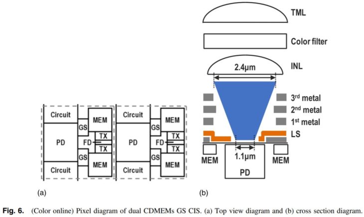
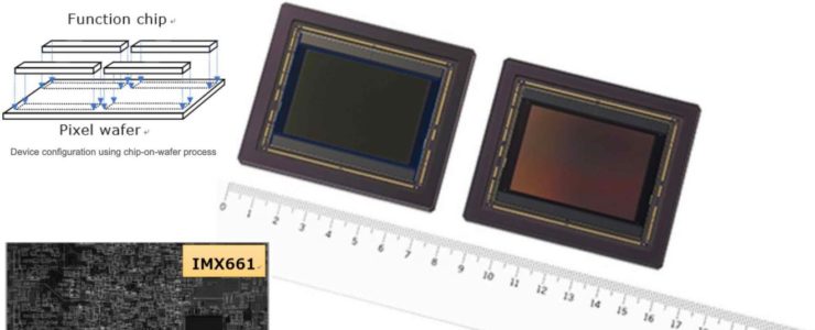
Tokyo, Japan — Sony Corporation announced today the upcoming release of a large format 56.73mm diagonal CMOS image sensor “IMX661” for industrial equipment with a global shutter function and the industry’s highest*1 effective pixel count of 127.68 megapixels.*2

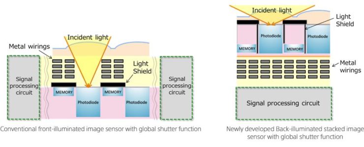
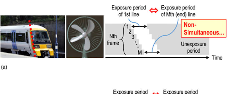
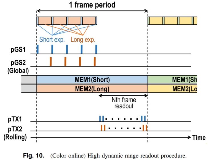
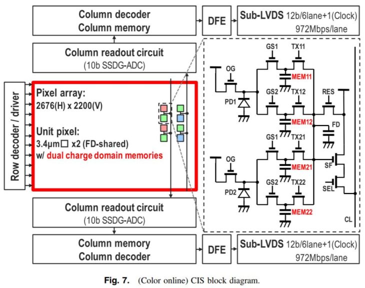
This product features an increased pixel count that yields an optical size nearly 10 times larger than the common 1.1-type image sensor corresponded to the C mount*3 for industrial equipment. It also features Sony’s original global shutter pixel technology “Pregius™”, which enables capture of motion distortion-free images. Furthermore, the Sony’s original device configuration and interface technology employed enable high-speed image readout at a data rate nearly four times faster*4 than conventional products.

Sony expects that the new sensor, when used in industrial equipment cameras for a wide variety of applications, will help to solve a variety of complex challenges, thereby contributing to the development of industry.

  • *1Among CMOS image sensors equipped with a global shutter. According to Sony research (as of announcement on March 9, 2021).
  • *2Based on image sensor effective pixel specification method.
  • *3The joining mechanism between lens and the camera body.
  • *4Compared to Sony’s “IMX253” 1.1 type, 12.37 effective megapixels CMOS image sensor equipped with a global shutter function.

Model name Sample: IMX661 3.6 type (56.73 mm diagonal) 127.68-effective-megapixel CMOS image sensor
Shipment date (planned)*5: April 2021(*5 The dates given for sample shipment date (planned) are for the color model. Black and white model samples will be available for shipment approximately one month later.

Needs for automation, labor-saving and other benefits of digital transformation continue to grow in recent years in various fields of industrial equipment. This has accelerated the adoption of cameras for a wide variety of applications, driving demand for CMOS image sensors with higher imaging performance.

The new product couples Sony’s Pregius technology with the 3.6-type (56.73mm diagonal) large optical size, delivering an increased pixel count and motion distortion-free imaging. The original device configuration, which employs a chip-on-wafer process, together with Sony’s original interface technology, enables high-speed readout nearly four times faster than conventional products*4 in full-pixel readout mode. This design delivers highly efficient imaging that captures a wide viewing angle with no motion distortion in a single imaging operation. It also improves recognition precision thanks to the high-resolution imaging and delivers a high level of processing performance. It can contribute to solutions for a variety of industrial equipment applications, for example, inspection processes for production of displays and electronic substrates, wide-area monitoring, and aerial photography, where its improved precision and quicker readout will help meet the need for a high level of productivity.

Click here to open the rest of the article

Industry News: Sony Develops A Stacked Global Shutter Sensor With Back-Illuminated Pixel

Global Shutter

Sony press release:

Sony Develops a Stacked CMOS Image Sensor Technology Using Sony’s Proprietary Global Shutter Function with Back-Illuminated Pixel Structure to Deliver Both High Imaging Performance and Miniaturization

Improves Productivity of Industrial Equipment for Smartification

Tokyo, Japan — Sony Corporation announced today that it has succeed in developing Pregius S, a stacked CMOS image sensor technology that employs Sony’s proprietary global shutter function with back-illuminated pixel structure to deliver both distortion-free, high imaging performance and miniaturization. The new sensor technology is intended for industrial equipment used in fields such as manufacturing, inspection, and logistics that require higher precision and higher processing speeds, in light of the trends in industrial advancement including factory smartification and automation.

Sony will introduce the new technology at Vision China Shanghai 2019 starting on March 20, 2019.

Conventional CMOS image sensors equipped with global shutter function temporarily store charge signals in the memory area located next to the photodiode to resolve image distortion (focal plane distortion) caused by the time shift due to the row-by-row readout. In front-illuminated CMOS image sensors, there is a wiring layer on the silicon substrate forming the photodiode, and with such a structure, the benefit is that it is easy to form a light shield for protecting the charge signal temporarily stored in the memory area from leaked light. For this reason, conventional CMOS image sensors with global shutter function have adopted a front-illuminated pixel structure. However, the wiring on top of the photodiode hinders the incident light, which creates an issue when attempting to miniaturize the pixels.

[expander_maker id=”2″ more=”Click to read the article” less=”Read less”]

In response to this, Sony has developed a proprietary pixel structure that achieves the global shutter function on a back-illuminated structure that has superior sensitivity characteristics, thereby resolving the issue of miniaturization. Normally, when pixels are miniaturized, the sensitivity and saturation characteristics deteriorate, but the new Sony technology enables a reduction in pixel size to 2.74 μm while maintaining performance of those characteristic, thereby achieving about 1.7 times higher resolution than conventional front-illuminated CMOS image sensors.*1 This makes it possible to measure and inspect objects in a wider area and with higher accuracy in manufacturing, inspection, logistics and other applications. Moreover, thanks to the high degree of freedom of the wiring layout of back-illuminated pixel structures, a high speed of about 2.4 times that of conventional*1 can be achieved, thereby contributing to significant productivity improvement, including shorter measurement and inspection process times. In addition, the sensor’s stacked structure makes it possible to mount various signal processing circuits, whereby it is possible to realize smart functions such as signal processing only for the necessary part of the measurement and inspection images in a smaller size compared to conventional sensors.*1 That, in turn, makes it possible to reduce the load of the subsequent processing and reduce the amount of data to be held on to, thereby contributing to the realization of highly efficient, energy-saving systems.

Going forward, Sony will work to develop products equipped with this stacked CMOS image sensor employing its proprietary global shutter function with back-illuminated pixel structure for various industrial applications and intelligent transportation systems, including development of derivatives for signal processing circuits to be mounted. Sony plans to start shipping sample units in the summer of 2019 or later.

Main Features

1) Proprietary global shutter function with back-illuminated pixel structure delivers both distortion-free high imaging performance and miniaturization

Sony developed a proprietary pixel structure that achieves a global shutter function on a back-illuminated structure that has superior sensitivity characteristics, delivering both high imaging performance and miniaturization. By miniaturizing the pixel size from the conventional*1 3.45 μm to 2.74 μm while maintaining sensitivity and saturation characteristics, Sony has achieved about 1.7 times higher resolution than the conventional front-illuminated 12 megapixels*2 CMOS image sensor,*1 thereby making it possible to perform measurement and inspection in a wider area and at a higher accuracy. Moreover, thanks to the high degree of freedom of the wiring layout of the back-illuminated pixel structure, it is possible to deliver high-speed performance of about 2.4 times that of the conventional technology*1, thereby contributing to significant productivity improvement such as shorter measurement and inspection process times.

2) Miniaturization and high functionality made possible with a stacked structure

The sensor’s stacked structure makes it possible to mount various signal processing circuits, thereby contributing to miniaturization and enhanced functions for CMOS image sensors. Incorporating the data optimization functions (smart ROI, self-trigger, compression processing, compositing, etc.) that extracts only necessary information from the image data, it is possible to reduce the load of the subsequent processing and reduce the amount of data to be held onto while achieving a smaller package compared to conventional sensors,*1 thereby contributing to the realization of highly efficient, energy-saving systems.

Going forward, Sony will leverage the technology of Pregius S to further enhance and expand functions for new industries, including development of derivatives for signal processing circuits to be mounted.

[/expander_maker]

Canon Working On Global Shutter Sensor With Dual Memory Pixels, Research Paper

Global Shutter

Canon published a research paper in the Japanese Journal of Applied Physics, named “A 3.4 μm pixel pitch global shutter CMOS image sensor with dual in-pixel charge domain memory” (by Masahiro Kobayashi, Hiroshi Sekine, Takafumi Miki, Takashi Muto, Toshiki Tsuboi, Yusuke Onuki, Yasushi Matsuno, Hidekazu Takahashi, Takeshi Ichikawa, and Shunpike Inoue).

From the paper’s abstract:

[expander_maker id=”2″ more=”Click to read the article” less=”Read less”]

In this paper, we describe a newly developed 3.4 μm pixel pitch global shutter CMOS image sensor (CIS) with dual in-pixel charge domain memories (CDMEMs) has about 5.3 M effective pixels and achieves 19 ke− full well capacity, 30 ke−/lxcenterdots sensitivity, 2.8 e- rms temporal noise, and −83 dB parasitic light sensitivity. In particular, we describe the sensor structure for improving the sensitivity and detail of the readout procedure. Furthermore, this image sensor realizes various readout with dual CDMEMs. For example, an alternate multiple-accumulation high dynamic range readout procedure achieves 60 fps operation and over 110 dB dynamic range in one-frame operation and is suitable in particular for moving object capturing. This front-side-illuminated CIS is fabricated in a 130 nm 1P4M with light shield CMOS process.

[via Image Sensors World] [/expander_maker]