Did You Know Nikon Designs its own Sensors?

Nikon

I didn’t.

Imaging Resource’s Dave Etchells had the rare chance to visit Nikon’s super-secret sensor design laboratory. But, wait, didn’t Sony manufacture the sensors in Nikon cameras?

So what is Nikon exactly doing? Say’s Etchells:

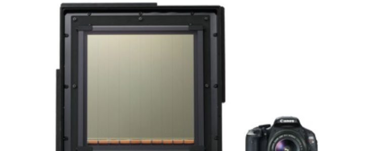
Companies designing chips of whatever sort generally rely on standard processes established by the “foundry” company that does the actual manufacturing. In these cases, the design process is “just” a matter of defining the layout of the devices on the chip. I say “just” though, because it’s far from a routine process to do this. The size and shape of transistors, photodiodes, resistors and capacitors determines their electrical characteristics, and there are loads of tradeoffs involved in balancing light-gathering efficiency, noise levels, readout speeds, on and on. A big trick is designing the pixels and readout circuitry so there’s as little “dead” (non-light-sensitive) area as possible, while maintaining readout speeds and minimizing power consumption.

Nikon designs its sensors and Sony manufactures them. The surprising thing here is how deep into details Nikon’s sensor design goes, let alone all the simulations and the testing. The reason Nikon is doing this, has to do

with being able to optimize the camera system as a whole, in ways that you can’t if you’re just using off-the shelf parts

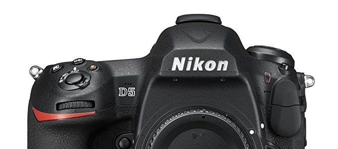
In other words: Nikon wants their sensors to be optimised for their lenses and to work at best with Nikon’s also in-house designed EXPEED image processing engine. The sensors featured in the Nikon D850 and Nikon D5 are an example of Nikon’s testing, simulation and overall sensor design.

To learn more about imaging sensors in general and about Nikon’s super-secret sensor design laboratory head over to Imaging Resource.

Canon Patent to reduce image noise generated by the magnetic field of image stabilisation unit

Canon Patent

Well, this is an interesting Canon patent application we spotted (20180164603), and it shows how much care Canon applies to details.

Some background information first. Simplifying it very much, the image stabilisation system of a lens is build on top of a vibration gyroscope sensor. The process of stabilising an image in the lens occurs through a image (shake) correcting unit. The correcting unit uses electromagnetic fields, generated by applying current to a coil.

The generated electromagnetic fields can influence the electronic circuitry and hence may degrade the image quality by generating noise in the image. Turns out that shielding the coil isn’t that easy.

If I got the patent right, it tries to reduce the magnetic field by clever use of non-magnetically conductive materials and shielding. From the patent literature:

According to one aspect of the present invention, there is provided an imaging lens including: a lens; an image shake correcting action unit provided movably in a direction perpendicular to an optical axis of the lens; a stationary unit for supporting the image shake correcting action unit; a permanent magnet provided on one of the image shake correcting action unit and the stationary unit and a coil provided on an other; a drive circuit for moving the image shake correcting action unit relative to the stationary unit; a mount section for being connected to an imaging unit having an imaging element; and a conductive member which is nonmagnetically conductive and disposed between the coil and the mount section so as to include a facing surface facing a surface formed by a binding wire of the coil and having a larger area than a surface formed by an inner periphery of the coil.

This patent application might go into production one day.

Other Canon patent applications we think might get into production in the next few years are these:

Canon explores large image sensors for academic and industrial application

Canon

Canon posted a technical article about the company’s efforts in researching large size image sensors. The sensor in the article below is 40 times the size of a 35mm CMOS sensor. Nothing you will see on Canon’s next mirrorless camera.

Canon press text:

The Potential to Open New Frontiers in Academic and Industrial FieldsCMOS Image Sensors

In addition to the image sensors used in its consumer-model digital cameras, Canon is exploring new potential in academic fields and industrial fields through the development of ultrahigh-sensitivity CMOS image sensors and ultrahigh-resolution CMOS image sensors.

The World’s Largest Ultrahigh-Sensitivity CMOS Image Sensor

A certain level of light is required when shooting with a digital camera or camcorder, and without it, images cannot be captured due to insufficient sensitivity.

In the pursuit of further improving the sensitivity of imaging elements, Canon has embraced the challenge of achieving higher levels of sensitivity and larger element sizes while maintaining high-speed readout performance, and has succeeded in developing the world’s largest class of CMOS image sensor measuring approximately 20 cm square. At present, the standard diameter of the silicon wafers on which CMOS sensors are fabricated is 12 inches (approx. 30 cm). As such, a 20-cm-square sensor is the largest size that can be manufactured based on these dimensions, and is equivalent to nearly 40 times the size of a 35 mm full-frame CMOS sensor.

Increasing the size of CMOS sensors entails overcoming such problems as distortion and transmission delays for the electrical signals converted from light. To resolve these issues, Canon not only made use of a parallel processing circuit, but also exercised ingenuity with the transfer method itself. As a result, the sensor makes possible the shooting of video at 60 frames per second with only 0.3 lux of illumination (approximately the same level of brightness as that generated by a full moon).

120-Megapixel Ultrahigh-Resolution CMOS Image Sensor

Canon has spent many years working to reduce the pixel size for CMOS image sensors. These efforts have led to astounding results, making possible a pixel size of 2.2 µm for a total of approximately 120 million pixels on a single sensor. The APS-H size (approx. 29 x 20 mm) CMOS sensor boasts approximately 7.5 times the number of pixels and 2.6 times the resolution of sensors of the same size featured in existing products.

This CMOS sensor performs parallel processing to support the high-speed readout of large volumes of pixels, and by modifying the method employed to control the readout circuit timing, Canon successfully achieved the high-speed readout of sensor signals. As a result, the sensor makes possible a maximum output speed of approximately 9.5 frames per second, supporting the continuous shooting of ultrahigh-resolution images.

Images captured with the ultrahigh-resolution CMOS sensor maintain high levels of definition and clarity even when cropped or digitally magnified. Accordingly, this sensor offers potential for a range of industrial applications, including cameras for shooting images for large-format poster prints, cameras for the image inspection of precision parts, aerospace cameras, and omnidirectional vision cameras.

The 120-megapixel ultrahigh-resolution performance of the Canon CMOS sensor may lead to unprecedented industrial applications that could only be imagined in the past.

[via Image Sensors World]

Canon enters sensor business, three high performance sensors on sale, 120MP inclusive

Canon

Three of Canon’s most advanced and specialised sensors are on sale to the public. This is no surprise as it was reported to be part of Canon’s plans back in 2016.

The sensors are a 120 Megapixel CMOS Sensor, a 5 Megapixel Global Shutter CMOS, and the 35MMFHDXS, 19μm Full HD CMOS Sensor. If you’re curious to learn more click here. In the past we reported extensively about these sensors.

The sensors can be purchased through Canon’s own authorized distributor Phase 1 Technology Corp.

Canon industrial sensors redefine high-performance with state-of-the-art technology, backed by decades of ongoing development and improvement. Featuring the 120 Megapixel CMOS sensor, the 5 Megapixel Global Shutter CMOS sensor, and the 35MMFHDXS CMOS sensor, Phase 1 Technology offers Canon’s most advanced industrial sensors.

For OEMs, solutions providers, vision integrators and others in search of advanced machine vision components, Canon’s powerful industrial sensors are equipped for a wide range of applications.

These kind of sensor gets used in surveillance tech, medical applications, and other specialised domains. Below you see some videos highlighting Canon’s sensors technology and performance.

The original Canon EOS M can shoot 2.5K raw video with Magic Lantern, and it’s impressing

Canon Eos M

Warning: the sd_uhs module referenced below is currently highly experimental and can destroy your sd card or camera. There have been instances of sd cards breaking. Magic Lantern does not recommend its use at the moment because of the risk involved.

I’m reporting this because Magic Lantern‘s work deserves it, and because I’m an old school hacker and can’t help getting excited by stuff like this. Computer science was made by this sort of guys, not by fancy dudes like Apple’s or the likes. I’ve been there since the beginning and I am pretty sure to understand the value of what these skilled hackers are doing.

So, here is another amazing hack by the Magic Lantern team, showcased by Synth & Sundry in the video below. It’s truly impressing: a Magic Lantern SD UHS overclock hack test on a the first Canon EOS M (2013). Shot at 2520×1080, 5x zoom mode, 24 fps, 12 bit lossless compressed raw using sd_uhs module. Not bad, eh?

It may be true that Canon cripples their tech when they want it, but still, this code hacking proofs what Canon’s sensor tech can deliver. Even on the so much disgraced original Canon EOS M (which I still proudly own and never will get rid off).

Again: do not try this if you don’t exactly know what you are doing. This is experimental stuff and it may seriously harm your camera, I do not encourage you to try to apply this hack.

Kudos Magic Lantern for the hacking! If you dare and want to know more, have a look at Magic Lantern’s download page.


We covered Magic Lantern’s work, and they have a forum where you can learn more.