Industry News: Sony Develops A Stacked Global Shutter Sensor With Back-Illuminated Pixel

Global Shutter

Sony press release:

Sony Develops a Stacked CMOS Image Sensor Technology Using Sony’s Proprietary Global Shutter Function with Back-Illuminated Pixel Structure to Deliver Both High Imaging Performance and Miniaturization

Improves Productivity of Industrial Equipment for Smartification

Tokyo, Japan — Sony Corporation announced today that it has succeed in developing Pregius S, a stacked CMOS image sensor technology that employs Sony’s proprietary global shutter function with back-illuminated pixel structure to deliver both distortion-free, high imaging performance and miniaturization. The new sensor technology is intended for industrial equipment used in fields such as manufacturing, inspection, and logistics that require higher precision and higher processing speeds, in light of the trends in industrial advancement including factory smartification and automation.

Sony will introduce the new technology at Vision China Shanghai 2019 starting on March 20, 2019.

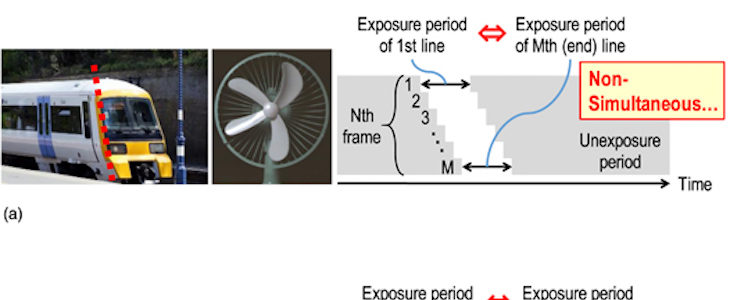
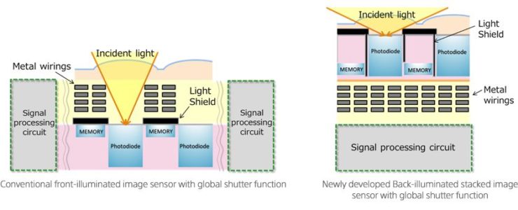
Conventional CMOS image sensors equipped with global shutter function temporarily store charge signals in the memory area located next to the photodiode to resolve image distortion (focal plane distortion) caused by the time shift due to the row-by-row readout. In front-illuminated CMOS image sensors, there is a wiring layer on the silicon substrate forming the photodiode, and with such a structure, the benefit is that it is easy to form a light shield for protecting the charge signal temporarily stored in the memory area from leaked light. For this reason, conventional CMOS image sensors with global shutter function have adopted a front-illuminated pixel structure. However, the wiring on top of the photodiode hinders the incident light, which creates an issue when attempting to miniaturize the pixels.

[expander_maker id=”2″ more=”Click to read the article” less=”Read less”]

In response to this, Sony has developed a proprietary pixel structure that achieves the global shutter function on a back-illuminated structure that has superior sensitivity characteristics, thereby resolving the issue of miniaturization. Normally, when pixels are miniaturized, the sensitivity and saturation characteristics deteriorate, but the new Sony technology enables a reduction in pixel size to 2.74 μm while maintaining performance of those characteristic, thereby achieving about 1.7 times higher resolution than conventional front-illuminated CMOS image sensors.*1 This makes it possible to measure and inspect objects in a wider area and with higher accuracy in manufacturing, inspection, logistics and other applications. Moreover, thanks to the high degree of freedom of the wiring layout of back-illuminated pixel structures, a high speed of about 2.4 times that of conventional*1 can be achieved, thereby contributing to significant productivity improvement, including shorter measurement and inspection process times. In addition, the sensor’s stacked structure makes it possible to mount various signal processing circuits, whereby it is possible to realize smart functions such as signal processing only for the necessary part of the measurement and inspection images in a smaller size compared to conventional sensors.*1 That, in turn, makes it possible to reduce the load of the subsequent processing and reduce the amount of data to be held on to, thereby contributing to the realization of highly efficient, energy-saving systems.

Going forward, Sony will work to develop products equipped with this stacked CMOS image sensor employing its proprietary global shutter function with back-illuminated pixel structure for various industrial applications and intelligent transportation systems, including development of derivatives for signal processing circuits to be mounted. Sony plans to start shipping sample units in the summer of 2019 or later.

Main Features

1) Proprietary global shutter function with back-illuminated pixel structure delivers both distortion-free high imaging performance and miniaturization

Sony developed a proprietary pixel structure that achieves a global shutter function on a back-illuminated structure that has superior sensitivity characteristics, delivering both high imaging performance and miniaturization. By miniaturizing the pixel size from the conventional*1 3.45 μm to 2.74 μm while maintaining sensitivity and saturation characteristics, Sony has achieved about 1.7 times higher resolution than the conventional front-illuminated 12 megapixels*2 CMOS image sensor,*1 thereby making it possible to perform measurement and inspection in a wider area and at a higher accuracy. Moreover, thanks to the high degree of freedom of the wiring layout of the back-illuminated pixel structure, it is possible to deliver high-speed performance of about 2.4 times that of the conventional technology*1, thereby contributing to significant productivity improvement such as shorter measurement and inspection process times.

2) Miniaturization and high functionality made possible with a stacked structure

The sensor’s stacked structure makes it possible to mount various signal processing circuits, thereby contributing to miniaturization and enhanced functions for CMOS image sensors. Incorporating the data optimization functions (smart ROI, self-trigger, compression processing, compositing, etc.) that extracts only necessary information from the image data, it is possible to reduce the load of the subsequent processing and reduce the amount of data to be held onto while achieving a smaller package compared to conventional sensors,*1 thereby contributing to the realization of highly efficient, energy-saving systems.

Going forward, Sony will leverage the technology of Pregius S to further enhance and expand functions for new industries, including development of derivatives for signal processing circuits to be mounted.

[/expander_maker]
Canon Working On Global Shutter Sensor With Dual Memory Pixels, Research Paper

Global Shutter

Canon published a research paper in the Japanese Journal of Applied Physics, named “A 3.4 μm pixel pitch global shutter CMOS image sensor with dual in-pixel charge domain memory” (by Masahiro Kobayashi, Hiroshi Sekine, Takafumi Miki, Takashi Muto, Toshiki Tsuboi, Yusuke Onuki, Yasushi Matsuno, Hidekazu Takahashi, Takeshi Ichikawa, and Shunpike Inoue).

From the paper’s abstract:

[expander_maker id=”2″ more=”Click to read the article” less=”Read less”]

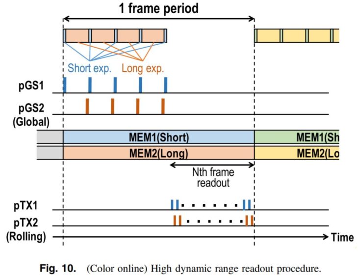
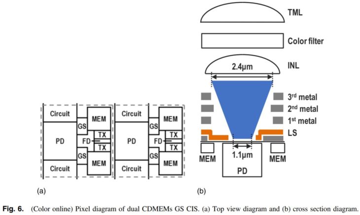
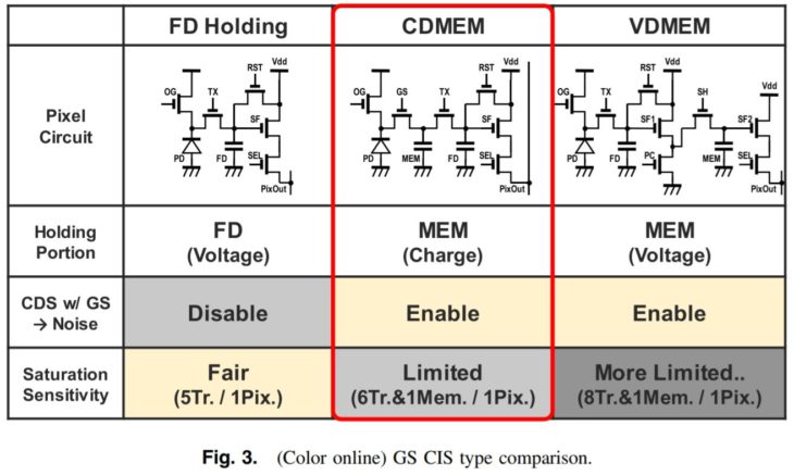
In this paper, we describe a newly developed 3.4 μm pixel pitch global shutter CMOS image sensor (CIS) with dual in-pixel charge domain memories (CDMEMs) has about 5.3 M effective pixels and achieves 19 ke− full well capacity, 30 ke−/lxcenterdots sensitivity, 2.8 e- rms temporal noise, and −83 dB parasitic light sensitivity. In particular, we describe the sensor structure for improving the sensitivity and detail of the readout procedure. Furthermore, this image sensor realizes various readout with dual CDMEMs. For example, an alternate multiple-accumulation high dynamic range readout procedure achieves 60 fps operation and over 110 dB dynamic range in one-frame operation and is suitable in particular for moving object capturing. This front-side-illuminated CIS is fabricated in a 130 nm 1P4M with light shield CMOS process.

[via Image Sensors World] [/expander_maker]

Latest Canon Patent Applications (Pop-UP EVF, Resin Mount, Hybrid EVF, Lenses and Sensor)

Canon Patent Applications

Here are the latest Canon patent applications.

Canon patent application 2019-023685 describes a pop-up EVF (Electronic ViewFinder). From the patent literature:

Since a display-device part and the eyepiece for magnifying it are needed EVF, when mounting on a compact camera, the place to arrange serves as problem. Since the large-sized external display device serves as a form which covers a camera back substantially, in order to look into EVF from the back face of a camera, an external display device must be avoided and arranged. A camera will enlarge only the part of EVF then. When it is going to avoid enlargement, an external display device must be made small and usability becomes less good. In order to correspond to these problems, there are some on which pop-up type EVF like the description to a Patent document 1 is mounted. 

EVF loading is realized without [ when using this inside a camera, being stored at the time of EVF non-use, without it functions as a finder by making it jump out to camera outside and miniaturizes an external display device, and ] enlarging a camera. 

Canon patent application 2019-023688 describes a resin (plastics) made lens mount:

Conventionally, although the camera mount of the camera with interchangeable lenses comprised a metallic material in consideration of durability, reliability and accuracy, etc., the camera mount which comprises a metallic material had the problem that things and component cost with heavy weight became high. 

The camera body which has the camera mount which comprised resin materials, such as a plastic, by improvement in the durability of engineering plastics or reliability and progress of forming technique is produced commercially these days. A weight saving and component cost reduction are attained because camera mount becomes a resin material.

Canon patent application 2019-020538 describes a hybrid optical and electronic viewfinder:

The present invention relates to the single-lens reflex camera which has an optical finder and an electronic finder, and relates to the change of the finder to which seeds responded as for the electronic device with which the especially single-lens reflex camera was equipped, or the optical element. 

In recent years, the single-lens reflex camera which has a finder which has arranged the optical-path dividing prism in the optical path of an optical finder in a single-lens reflex camera, and has arranged the display device which becomes the equivalent position from a liquid crystal panel etc. optically with a focus detecting plate is known. 

Canon patent application 2019-020679 describes the optical formula for a RF 100-400mm lens (for EOS R systems):

Focal distance 102.21 195.97 389.86 ​
F number 3.83 4.93 5.85 
Half angle of view (degree) 11.95 6.30 3.18 
Image height 21.64 21.64 21.64 
Lens total length 204.85 250.29 291.30 
BF 4.31 31.68 97.49

Canon patent application 2019-017065 describes a photon counting image sensor.

Canon patent application 2019-0052781 discusses how to improve the reliability of tilt-shift lenses.

That’s all for now; patent round-up source: Canon News

More Canon patent applications are listed here. Some particularly interesting patent applications we think might get into production in the next few years are these:

Canon Set To Use A Sony Back-Illuminated APS-C Sensor In Future Cameras?

Sony

Another weird rumor to report.

It’s suggested Canon might use the new Sony IMX571 image sensor in an upcoming APS-C camera system. No hints if it will be a MILC or a DSLR.

The Sony IMX571 sensor is back-illuminated, has a resolution of 26MP and does 16 frame per second.

Despite Canon used Sony sensors in the past for their Powershot cameras, we do not think a Sony sensor will be featured on DSLR or mirrorless camera. We did not get any suggestion pointing in this direction.

Stay tuned.

Macnica Americas to Distribute Canon’s Super Specialised CMOS Image Sensors

35MMFHDXSCA Image Sensors

Canon’s super specialised sensors are now available for industrial applications. Macnica will be the distributor.

Press release:

Macnica Americas to Distribute Canon CMOS Image Sensors

Advanced CMOS Technology Ideal for High Performance Industrial Cameras Up to 120 MP

MELVILLE, N.Y., November 7, 2018 – Canon U.S.A., a leader in digital imaging solutions, and Macnica Americas, Inc., the North American subsidiary of Macnica, Inc., a $5B global leader in technology product distribution, today announced that Macnica Americas has been appointed an authorized distributor of Canon’s advanced CMOS sensors for the United States and Canada.

“Canon’s sensors offer incredible performance that Macnica Americas is excited to make available to our camera manufacturer customers,” said Akinobu Miyoshi, CEO of Macnica Americas.

“Imaging expertise is the core of Canon’s heritage and the success of the CMOS sensors in our product line is an example of that expertise,” said Kazuto Ogawa, president and chief operating officer, Canon U.S.A., Inc. “Appointing Macnica Americas as an authorized distributor will expand our reach by offering this state-of-the-art technology to industrial camera manufacturers looking to innovate their solutions now and in the future.”

Canon offers the following high performance CMOS sensors targeted at industrial, medical and scientific applications:

  • 3U5MGXS – A 5 Megapixel, 2/3-inch global shutter image sensor, that offers 120 frames per second (fps) readout at low power, targeted at machine vision applications.
  • 35MMFHDXSCA – Larger than full frame, this 2.76 Megapixel low-light sensor with 19 mm pixel pitch is ideal for ultra low-light cameras used in defense, surveillance or astronomy applications.
  • 120MXS – A stunning 120 megapixel ultra high-resolution sensor (approx. 60x the resolution of HD), in an APS-H format, enables high resolution imaging at 9.4 fps. Target camera applications for this sensor include inspection, aerial mapping, life sciences, digital archiving and transportation industries.

Canon’s CMOS image sensors are available in a range of options including color (RGB) and monochrome. For more details, please click on the link.


About Macnica Americas

Macnica Americas is the North American Division of Macnica, Inc. a $5B global leader in technology product distribution, high-touch support and complex design services, with global headquarters in Yokohama, Japan. Macnica Americas serves OEM companies, particularly those specializing in creating innovative video, imaging, networking and storage products. Macnica Americas’ headquarters are located in San Diego, with offices in San Jose, Dallas, Chicago, and Boston, and representatives throughout the United States and Canada.

Canon EOS R and Nikon Z7 Can Not Beat Sony a7 III When It Comes To Pure Dynamic Range Sensor Figures

Canon Eos R

At Photons To Photo you can compare sensor figures of various camera.

As you can see in the image above, the Sony a7 III is still the champion of pure sensor performance, beating the Canon EOS R and Nikon Z7 on dynamic range measures.. Which is a pity especially for Nikon, since they are using a sensor made by Sony.

Canon, designing and manufacturing their own sensors. gets closer to Sony’s sensor performance as ISO gets higher (but around ISO 32000 Sony gets the edge again).

Sensor performance figures do not tell the whole story, and the differences shown in the graph above are really minimal. When it comes to ergonomics, lens ecosystem, reliability, customer support, weather sealing, and whatever counts beyond sensor performance, Canon is still the the alpha dog in the pack.