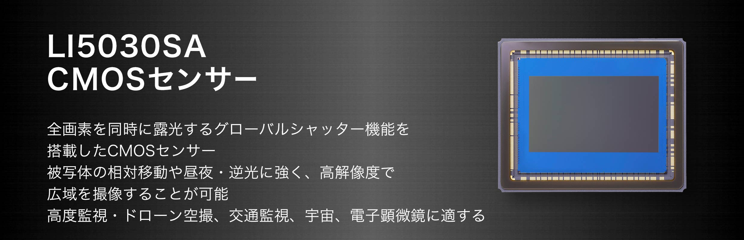
Canon has released the LI5030SA, an imaging sensor for industrial and scientific applications, like microscopes, automation, surveillance, machine vision, to name a few.
The Canon LI5030 features a global shutter that simultaneously exposes all 19MP of the sensor’s resolution. Perfect for subject moving with high speed, like propeller blades (seen in countless videos to demonstrate artefacts caused by a rolling shutter). he sensor delivers 5688 x 3334 video resolution at 57.99 fps and 12bit via 24 channels of digital signal output. The LI5030SA family has these siblings: LI5030SAC (color), LI5030SAI (RGBIR, raffic monitoring cameras and industrial cameras that can simultaneously capture visible and near infrared areas), LI5030SAM (monochrome), and LI5030SAN (Naked, no microlens or color filter for electron microscopes and X-ray detection cameras).
Latest rumor has it that Canon might be set to release more cameras featuring a stacked sensor.
Stacked sensor was first introduced with the Canon EOS R3. The source of the rumor claims that Canon will release three new cameras with a stacked sensor. One might be the fabled EOS R1, another one might be the EOS R5 Mark II. Don’t get too excited, though.
The rumor doesn’t come with any consolidating argument nor with a timeline or release date. It’s all very speculative and we recommend you take it with a grain of salt. if ever, these sensors will be seen in 2024.
Sony announced the development of a new image sensor with 2-Layer transistor pixels.
Sony press release:
Sony Develops World’s First*1 Stacked CMOS Image Sensor Technology with 2-Layer Transistor Pixel
Widens Dynamic Range and Reduces Noise by Approximately Doubling*2 Saturation Signal Level*3
*1: As of announcement on December 16, 2021.
*2: Based on comparison, on a one square μm equivalent basis, between existing image sensor and the new technology applied to Sony’s back-illuminated CMOS image sensor; as of announcement on December 16, 2021.
*3: A single pixel’s maximum electron storage capacity.
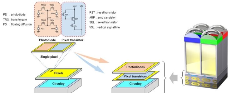
Sony Semiconductor Solutions Corporation (“Sony”) has succeeded in developing the world’s first*1 stacked CMOS image sensor technology with 2-Layer Transistor Pixel. Whereas conventional CMOS image sensors’ photodiodes and pixel transistors occupy the same substrate, Sony’s new technology separates photodiodes and pixel transistors on different substrate layers. This new architecture approximately doubles*2 saturation signal level*3 relative to conventional image sensors, widens dynamic range and reduces noise, thereby substantially improving imaging properties. The new technology’s pixel structure will enable pixels to maintain or improve their existing properties at not only current but also smaller pixel sizes.
Sony announced this breakthrough at the IEEE International Electron Devices Meeting that started on Saturday, December 11, 2021.
Stacked CMOS image sensor architectures
A stacked CMOS image sensor adopts a stacked structure consisting of a pixel chip made up of back-illuminated pixels stacked atop a logic chip where signal processing circuits are formed. Within the pixel chip, photodiodes for converting light to electrical signals, and pixel transistors for controlling the signals are situated alongside each other on the same layer. Increasing saturation signal level within form-factor constraints plays an important role in realizing high image quality with wide dynamic range.
Sony’s new architecture is an advancement in stacked CMOS image sensor technology. Using its proprietary stacking technology, Sony packaged the photodiodes and pixel transistors on separate substrates stacked one atop the other. In conventional stacked CMOS image sensors, by contrast, the photodiodes and pixel transistors sit alongside each other on the same substrate. The new stacking technology enables adoption of architectures that allow the photodiode and pixel transistor layers to each be optimized, thereby approximately doubling saturation signal level relative to conventional image sensors and, in turn, widening dynamic range.
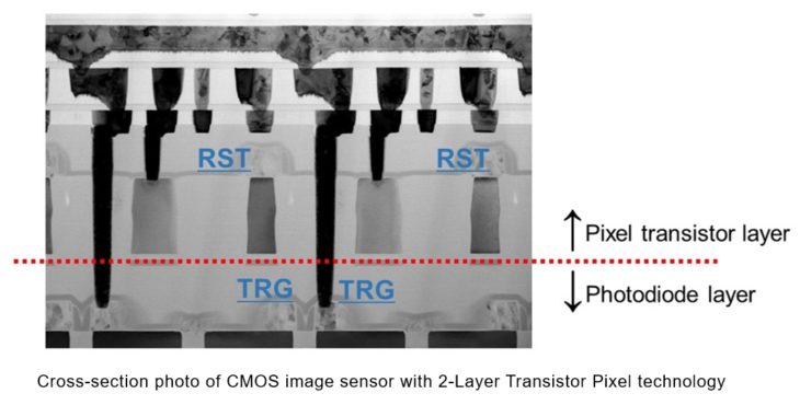
Additionally, because pixel transistors other than transfer gates (TRG), including reset transistors (RST), select transistors (SEL) and amp transistors (AMP), occupy a photodiode-free layer, the amp transistors can be increased in size. By increasing amp transistor size, Sony succeeded in substantially reducing the noise to which nighttime and other dark-location images are prone. The widened dynamic range and noise reduction available from this new technology will prevent underexposure and overexposure in settings with a combination of bright and dim illumination (e.g., backlit settings) and enable high-quality, low-noise images even in low-light (e.g., indoor, nighttime) settings. Sony will contribute to the realization of increasingly high-quality imaging such as smartphone photographs with its 2-Layer Transistor Pixel technology.
Canon is set to establish a new CMOS sensor manufacturing factory at Hiratsuka Plant, Japan. The production will fulfill primarily Canon’s own imaging sensor needs but they may also sell to third parties in the future.
The report comes from Newswitch and as spotted by Digital Camera Info, which summarizes what it is about (emphasis mine):
Canon will utilize part of the site of the Hiratsuka Plant (Hiratsuka City, Kanagawa Prefecture) to build a new CMOS image sensor manufacturing building. The investment amount is over 21 billion yen. Scheduled to start operation in July 2023. In addition to increasing the production capacity of CMOS image sensors installed in its own products such as cameras, it will also respond to growing demand for external sales.
Originally, Canon produced CMOS image sensors for the purpose of in-house production for its own cameras, but started selling them outside a few years ago. It is used in applications such as surveillance cameras and inspection equipment.
I wonder if this plant will also produce imaging sensors for consumer cameras. Guess it will, given the global supply chain issues.
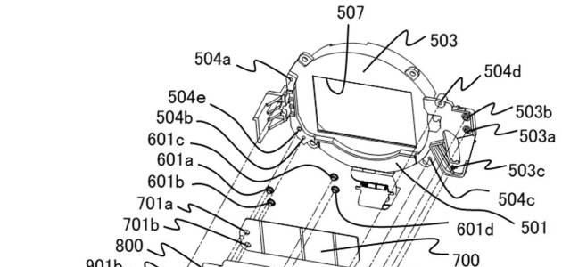
Here is an interesting Canon patent: a mechanism to protect the sensor from dust and dirt while no lens is attached.
Canon patent application P2021-103248A discusses a technology able to protect the imaging sensor of a camera from dust and dirt when no lens is mounted (e.g. while changing lens). From the patent literature:
PROBLEM TO BE SOLVED: To provide an image pickup apparatus with a barrier mechanism capable of being arranged in a small space while avoiding interference with components other than the barrier mechanism.
When the interchangeable lens is removed from the interchangeable lens type image pickup device (camera), dust may enter the camera through the opening of the mount and adhere to the image pickup element. Therefore, the image pickup device may be equipped with a barrier mechanism that protects the image pickup element by closing the opening of the mount. Patent Document 1 discloses a barrier mechanism configured such that a barrier closes an opening of a mount when the lens is not attached and the barrier is opened by rotation when the lens is attached.
As asobinet.com rightfully notices, the patent is not for a “compact shutter unit”, as wrongfully stated by some sites:
Some overseas information sites misrepresent it as a “compact shutter unit”, but it is just a shutter mechanism for “sensor protection” and a technology to prevent dust from adhering to the sensor when changing lenses. is. The compact sensor barrier seems to be a space-saving design that suppresses interference with other parts.
More Canon patents are listed here. Some particularly interesting patent applications we think might get into production are these:
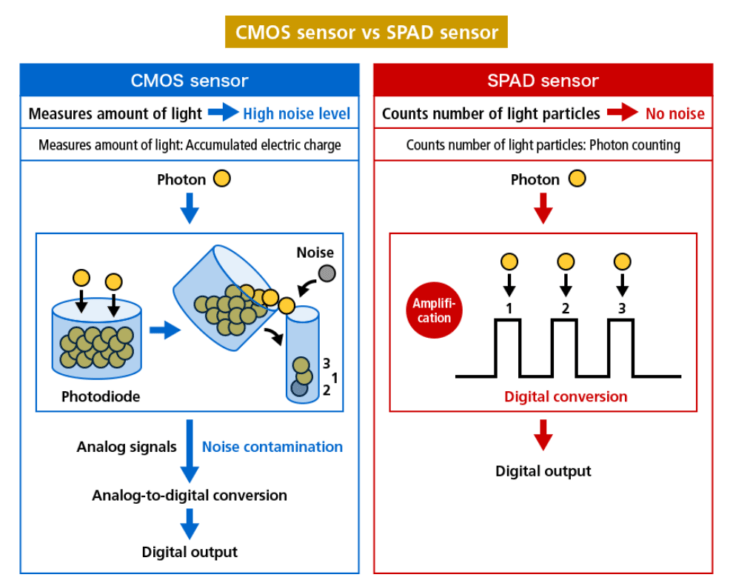
Canon published a technical article about the world’s first 1-megapixel SPAD image sensor. A groundbreaking image sensor and distance measurement sensor that will be the eyes of the future.
The advanced technology discussed in the Canon article is for applications involving augmented and virtual reality, ultra-high frames-per-second shooting speeds, robot automation, computer vision, and driverless vehicles. Here are some excerpts from the article:
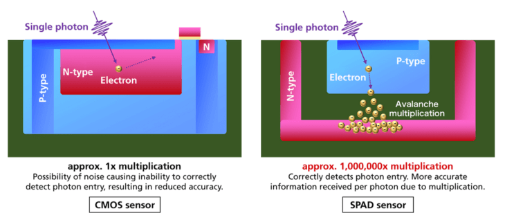
Both SPAD and CMOS sensors make use of the fact that light is made up of particles. However, with CMOS sensors, each pixel measures the amount of light that reaches the pixel within a given time, whereas SPAD sensors measure each individual light particle (i.e., photon) that reaches the pixel. Each photon that enters the pixel immediately gets converted into an electric charge, and the electrons that result are eventually multiplied like an avalanche until they form a large signal charge that can be extracted.
[…] it was considered difficult to create a high-pixel-count SPAD sensor. On each pixel, the sensing site (surface area available for detecting incoming light as signals) was already small. Making the pixels smaller so that more pixels could be incorporated in the image sensor would cause the sensing sites to become even smaller, in turn resulting in very little light entering the sensor, which would also be a big problem.[…] Canon incorporated a proprietary structural design that used technologies cultivated through production of commercial-use CMOS sensors. This design successfully kept the aperture rate at 100% regardless of the pixel size, making it possible to capture all light that entered without any leakage, even if the number of pixels was increased. The result was the achievement of an unprecedented 1,000,000-pixel SPAD sensor.
Canon sees many applications for their new and revolutionary image sensor:
In the fields of AR (augmented reality) and VR (virtual reality), which involve superimposing virtual images on top of real ones, being able to use the SPAD sensor to speedily obtain accurate three-dimensional spatial information enables more precise alignment of positions in real time. There are also high expectations for the application of SPAD sensors in solving one of the greatest challenges in designing driverless vehicles: the measurement of distances between a vehicle and the people and objects in its vicinity.
The article is very interesting and if you are into these technologies we recommend you give the article a try. The whole thing was spotted by Image Sensors World. More tech stuff is listed here.
This website or its third-party tools use cookies, which are necessary to its functioning and required to achieve the purposes illustrated in the cookie policy. If you want to know more or withdraw your consent to all or some of the cookies, please refer to the cookie policy. By closing this banner you agree to the use of cookies.